From instant UPI payments on your phone to life-saving hospital equipment, semiconductor chips quietly run our daily lives. Yet, total reliance on imports means a single overseas glitch can delay our car deliveries and drive-up gadget prices overnight.
To change this, India is investing billions to build domestic chip plants. The semiconductor industry in India 2030 roadmap aims to make the country a self-reliant tech hub—but can India truly pull it off against global giants? This article breaks down real ground investments, key predictions, and the impact on AI, cars, and jobs.
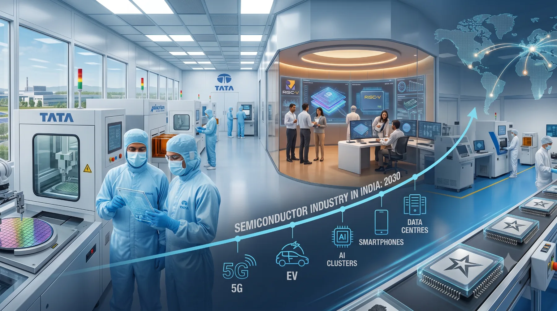
What is a Semiconductor? The Nano-Brain Behind Modern Technology
A semiconductor is a material (predominantly silicon) whose electrical conductivity falls between a conductor (like copper) and an insulator (like glass).
By precisely etching billions of microscopic switches called transistors onto a sliver of silicon, engineers create an integrated circuit (IC), or microchip. These chips process binary code ($0$s and $1$s), serving as the foundational building block for future technology India is adopting—from basic LED bulbs to autonomous defense satellites.
Confirmed Ground Reality: Mega Fabs and Packaging Units Under Construction
To separate the real growth of chip manufacturing India from speculative headlines, look at the concrete projects backed by the government's 50% fiscal capital support through the India Semiconductor Mission (ISM):
Tata Electronics & PSMC (Dholera, Gujarat): India's first commercial mega wafer fab. Built in partnership with Taiwan's PSMC with a ₹91,000 crore ($11B) outlay, this plant targets high-volume mature nodes (28nm, 40nm, 90nm) for automotive, power switches, and consumer logic. With multi-state procurement involving semiconductor equipment imports and interstate logistics, businesses must closely manage tax compliance by understanding how to calculate CGST and SGST with IGST rules .
Micron Technology (Sanand, Gujarat): A $2.75 billion advanced Assembly, Testing, Marking, and Packaging (ATMP/OSAT) facility. It is dedicated to assembling and packaging domestic and global supplies of DRAM and NAND memory chips.
Tata Semiconductor Assembly & Test (Morigaon, Assam): A ₹27,000 crore ($3B+) project focusing on sophisticated wire-bond and flip-chip packaging for electric vehicles and mobile electronics.
CG Semi JV (Sanand, Gujarat): A joint venture involving CG Power, Renesas (Japan), and Stars Microelectronics, building specialized packaging lines for industrial power chips and automotive microcontrollers.
Kaynes Semicon (Sanand, Gujarat): An operational and expanding power semiconductor and packaging hub catering to high-volume industrial units.
Chip Design and VLSI: India's Unmatched Global Moat
While the world views India as a newcomer to hardware manufacturing, the nation has quietly anchored global chip architecture for decades.
The Global Engineering Backbone
Nearly 20% of the world's semiconductor design workforce is based out of Bengaluru, Hyderabad, Noida, and Pune. Global giants like NVIDIA, Qualcomm, Intel, AMD, and MediaTek design their most complex microarchitectures using Indian engineers. While Tier-1 tech hubs lead deep VLSI research, the broader digital engineering landscape across eastern India is also expanding rapidly through local technical agencies like a trusted Website Development Company in Asansol .
Rise of Indigenous RISC-V Startups
Through the government's Design-Linked Incentive (DLI) scheme, homegrown fabless startups like InCore Semiconductors and Mindgrove Technologies are commercializing open-source RISC-V microcontrollers. These domestic chips are already replacing imports in electricity smart meters, industrial sensors, and IoT devices.
Sector-Wise Transformation: What Changes for End Users by 2030?
The maturation of the semiconductor industry in India directly shields domestic consumer sectors from foreign supply chokepoints:
| Heading | Heading | Current Status (Import Reliance) | 2030 Reality (Domestic & Packaged Chips) | |
|---|---|---|---|---|
| Smartphones | 100% of processors, PMICs, and RF modules imported | Packaged memory, display drivers, and power ICs sourced locally, lifting domestic value addition past 35%. | ||
| Electric Vehicles & Auto | Delivery delays driven by global automotive microcontroller shortages | Dholera Fab and local OSAT units supply automotive-grade chips directly to domestic automakers. | ||
| Data Centres & Cloud | Core server processors and enterprise SSDs imported | Edge-computing modules and domestic networking interface chips assembled locally. | ||
| Artificial Intelligence (AI) | Complete reliance on imported GPU hardware |
| Development of custom sovereign edge-AI application-specific ICs (ASICs) for smart city and telecom infrastructure. | |
| Development of custom sovereign edge-AI application-specific ICs (ASICs) for smart city and telecom infrastructure. |
To understand how this affects the auto space, read our breakdown of Electric Vehicle supply chains in India .
High-Tech Manufacturing and Job Creation Opportunities
Semiconductor fabrication functions as an economic multiplier: one core cleanroom role generates 4 to 5 allied jobs across the industrial supply chain.
Specialized Engineering Roles
The market demand for VLSI design, physical verification, FPGA prototyping, and packaging architecture specialists is on track to double by 2030.
Cleanroom Operations and Equipment Technicians
Operating high-precision lithography and etching tools requires chemical engineers, vacuum system specialists, and cleanroom technicians trained in zero-defect standards.
Allied Chemical and Industrial Supply Chains
A fab cannot run in isolation; hundreds of medium and small enterprises (MSMEs) will find fresh business delivering ultra-pure industrial gases, precision chemicals, and cleanroom equipment. To scale these operational workflows efficiently, many vendors are adopting the right tools outlined in our guide on the Software Stack an Indian Small Business Actually Needs .
Realistic Predictions: Where Will India Stand in 2030?
It is vital to distinguish realistic milestones from ungrounded hype:
Dominance in Mature Nodes, Not Sub-3nm: India will not manufacture 2nm or 3nm cutting-edge smartphone processors by 2030—those require decades of extreme ultraviolet (EUV) expertise. However, 28nm to 65nm legacy nodes comprise 70% of global demand (cars, home appliances, power grids, satellites), and this is precisely where India is set to compete.
Global Packaging Alternative: India is positioned to become a prime "China+1" destination for OSAT and advanced packaging, serving as a key alternate hub alongside Southeast Asia.
Persistent Structural Challenges: Maintaining uninterrupted 24/7 power, securing millions of liters of ultra-pure water daily, and relying on foreign toolmakers (ASML, Applied Materials) will remain critical operational hurdles.
Conclusion
By 2030, India will not replace Taiwan or South Korea at the cutting-edge of 2nm fabrication, but it does not need to. By anchoring its strategy in high-volume mature nodes, rapid OSAT expansion, and an already dominant chip-design workforce, the nation is steadily carving out an irreplaceable role in the global supply chain. The transition from an import-dependent consumer to a sovereign semiconductor producer is no longer just policy on paper—it is an unfolding industrial reality that will define India's economic resilience for decades to come.
Frequently asked questions
Will India manufacture flagship smartphone processors by 2030?
No, flagship phone processors require leading-edge nodes (3nm/4nm) controlled by foundries like TSMC. However, India will produce and package secondary phone chips, including power management ICs, display drivers, and memory modules.
What is the primary focus of the India Semiconductor Mission?
The India Semiconductor Mission (ISM) provides up to 50% capital expenditure support to companies establishing silicon wafer fabs, display fabs, and OSAT/ATMP packaging facilities across the country.
: Why are mature nodes (28nm+) important for India?
Mature nodes drive over 70% of the world's electronics volume. They run essential systems in electric vehicles, trains, power grids, industrial automation, and household gadgets, offering India an immediate market without the prohibitive costs of leading-edge research.
What is the difference between a Wafer Fab and an OSAT unit?
A Wafer Fab makes the raw chip from scratch by etching transistors onto silicon wafers. An OSAT unit cuts that wafer, tests the individual chips, and puts them into protective packages with pins so they can be soldered onto devices.